- 您现在的位置:买卖IC网 > Sheet目录1233 > NB4N11MDTEVB (ON Semiconductor)BOARD EVAL FOR NB4N11MD
�� �
�
�NB4N11MDTEVB�
�NC�
�SMA_GND�
�NC�
�SMA_GND�
�V� CC�
�V� CC�
�V� EE�
�V� EE�
�V� EE�
�V� CC�
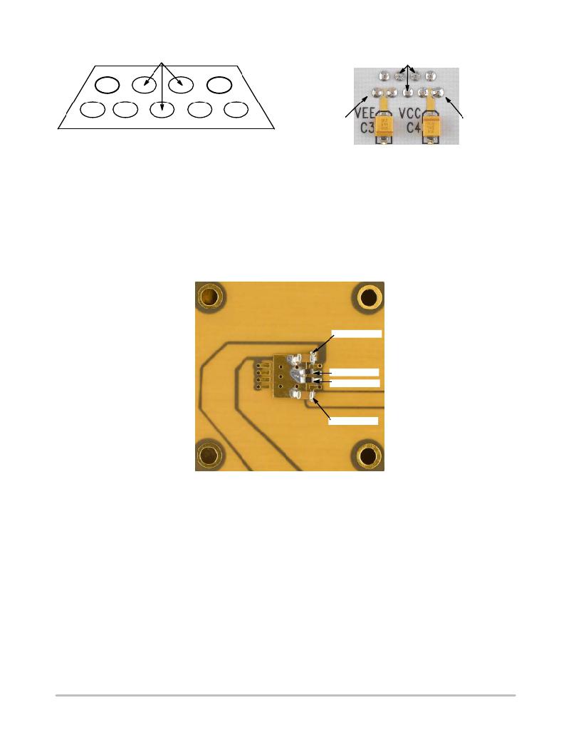
�C3� =� 10� m� F;� C4� =� 10� m� F�
�Figure� 4.� Power� Supply� Connector� ?� 9� Pin� Side�
�View� (Left)� and� PCB� Top� View� (Right)�
�Stimulus� (Generator)� Termination�
�All� ECL� outputs� need� to� be� terminated� to� V� TT� (V� TT� =�
�V� CC� –� 2.0� V� =� GND)� via� a� 50� W� resistor.� The� current� board�
�design� utilizes� the� space� for� placement� of� the� external�
�termination� resistors.� (More� information� on� termination� is�
�provided� in� AN8020).� The� 0402� chip� resistor� pads� are�
�provided� on� the� bottom� side� of� the� evaluation� board.� Solder�
�the� chip� resistors� to� the� bottom� side� of� the� board� between� the�
�appropriate� input� of� the� device� pin� pads� and� the� ground� pads�
�as� shown� in� Figure� 5� (for� split� power� supply� setup,� PCB� is�
�assembled� in� this� configuration).�
�C1� =� 0.01� m� F�
�R2� =� 50� W�
�R1� =� 50� W�
�C2� =� 0.01� m� F�
�Figure� 5.� Expanded� Bottom� View�
�Likewise� for� CML� outputs,� CML� stimulus� signal� need� to�
�be� terminated� to� V� CC� via� a� 50� W� resistor.� To� accomplish� this�
�configuration� the� external� termination� resistor� has� to� be�
�moved� from� SMA_GND� ring� to� V� CC� ring� on� the� bottom� of�
�the� board.�
�For� the� LVDS� configuration� Input� pin� pads� of� the� D0� or�
�D1� input� has� to� be� shorted� using� 100� W� resistor� across�
�differential� lines.�
�oscilloscope� to� be� used� as� a� termination� of� the� signals� (in�
�split� power� supply� setup� SMA_GND� as� a� system� ground,�
�V� CC� ,� and� V� EE� are� varied;� see� Table� 1,� Power� Supply� Levels).�
�Board� Components� Configuration�
�The� NB4N11MDTEVB� evaluation� board� requires� six�
�side� SMA� connectors.� Placement� locations� are� described� in�
�the� Table� 2� below.�
�DUT� Termination�
�For� standard� lab� setup� and� test,� a� split� (dual)� power� supply�
�is� required� enabling� the� 50� W� internal� impedance� in� the�
�http://onsemi.com�
�3�
�发布紧急采购,3分钟左右您将得到回复。
相关PDF资料
NB4N441MNGEVB
BOARD EVAL NB4N441MNG
NB4N507ADEVB
BOARD EVAL FOR BBG NB4N507AD
NB4N855SMEVB
CUSTOMER EVALUATION BRD
NB6L11MMNGEVB
BOARD EVAL NB6L11MMN CLK BUFFER
NB6L239MNEVB
BOARD EVAL BBG NB6L239MND
NB7L32MMNEVB
BOARD EVAL FOR NB7L32MM
NB7N017MEVB
BOARD EVAL BBG NB7N017MMN
NC2003SR
STAND NOTEBOOK W/2FANS USB
相关代理商/技术参数
NB4N11MDTG
功能描述:时钟缓冲器 MLTLVL IN-CML RECBUF RoHS:否 制造商:Texas Instruments 输出端数量:5 最大输入频率:40 MHz 传播延迟(最大值): 电源电压-最大:3.45 V 电源电压-最小:2.375 V 最大功率耗散: 最大工作温度:+ 85 C 最小工作温度:- 40 C 封装 / 箱体:LLP-24 封装:Reel
NB4N11MDTR2G
功能描述:时钟缓冲器 MLTLVL IN-CML RECBUF RoHS:否 制造商:Texas Instruments 输出端数量:5 最大输入频率:40 MHz 传播延迟(最大值): 电源电压-最大:3.45 V 电源电压-最小:2.375 V 最大功率耗散: 最大工作温度:+ 85 C 最小工作温度:- 40 C 封装 / 箱体:LLP-24 封装:Reel
NB4N11SMNG
功能描述:时钟缓冲器 LVDS FANOUT BUFF/ TRANS RoHS:否 制造商:Texas Instruments 输出端数量:5 最大输入频率:40 MHz 传播延迟(最大值): 电源电压-最大:3.45 V 电源电压-最小:2.375 V 最大功率耗散: 最大工作温度:+ 85 C 最小工作温度:- 40 C 封装 / 箱体:LLP-24 封装:Reel
NB4N11SMNR2G
功能描述:时钟缓冲器 LVDS FANOUT BUFF/ TRANS RoHS:否 制造商:Texas Instruments 输出端数量:5 最大输入频率:40 MHz 传播延迟(最大值): 电源电压-最大:3.45 V 电源电压-最小:2.375 V 最大功率耗散: 最大工作温度:+ 85 C 最小工作温度:- 40 C 封装 / 箱体:LLP-24 封装:Reel
NB4N121K
制造商:ONSEMI 制造商全称:ON Semiconductor 功能描述:3.3V Differential In 1:21 Differential Fanout Clock Driver with HCSL level Output
NB4N121KMN
制造商:ONSEMI 制造商全称:ON Semiconductor 功能描述:3.3V Differential In 1:21 Differential Fanout Clock Driver with HCSL level Output
NB4N121KMNG
功能描述:时钟缓冲器 UTL TSMC 1:21 FANOUT HCSL RoHS:否 制造商:Texas Instruments 输出端数量:5 最大输入频率:40 MHz 传播延迟(最大值): 电源电压-最大:3.45 V 电源电压-最小:2.375 V 最大功率耗散: 最大工作温度:+ 85 C 最小工作温度:- 40 C 封装 / 箱体:LLP-24 封装:Reel
NB4N121KMNGEVB
功能描述:BOARD EVAL NB4N121 FANOUT BUFFER RoHS:是 类别:编程器,开发系统 >> 评估演示板和套件 系列:* 产品培训模块:Obsolescence Mitigation Program 标准包装:1 系列:- 主要目的:电源管理,电池充电器 嵌入式:否 已用 IC / 零件:MAX8903A 主要属性:1 芯锂离子电池 次要属性:状态 LED 已供物品:板